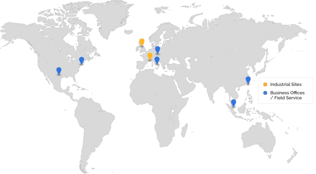
Demo Lab and Foundry
Ion Implantation
IBS is the perfect partner for supporting your ion implantation needs.
Whether it is production or R&D, IBS has a solution to fit all customer’s needs
Beamline implantation services
Production:
- Standard Processing: Fabless, ion implanter-less or additionnal production capacity without CapEx heavy investment
- Back-up: Breakdown, temporary overlay, wafer size upgrade…
R&D implantation:
- Specific processes: product development, test & evaluation
- Various substrates, shapes
- Exotic species
- Heated/cooled, various angles…
SiC implantation:
- From room temperature to +600 °C implant
- From samples to 6” wafer
- Si, B, Al, N, C, P and much more
- From 5 to 400 keV
- Specific SiC ion implant simulations
Plasma Immersion Ion Implant services (PIII)
PULSION®
- Available species:
• Doping: AsH3, PH3, BF3, B2H6
• Material modification: Ar, H2, He, CH4, SiH4, SiF4, Al, CF4, C2H2… - Wafer size: from samples up to 300 mm
- From medium to high doses
- Extremely low to medium acceleration voltage: 50 V – 20 kV
- Conformal doping for 3D
PIII & laser annealing combination
- Annealing (and diffusion) depth is controlled very precisely
- Room temperature doping
- Wafer integrity
- Junction depth from 10 nm to 15 nm
- Application: Back side implantation, power components
Ion implanters tailored to your needs
Demo Request
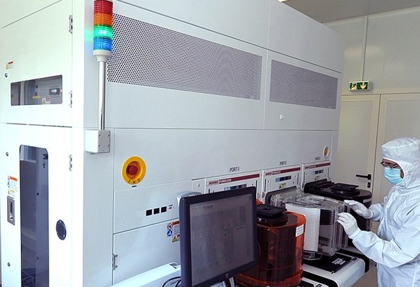
Experience the precision of IBS technology before integration.
We invite our customers to validate their specific doping requirements at our state-of-the-art demo facility in Peynier, France. Our experts work closely with your R&D teams to perform process evaluations on your own wafers.
Proof of Concept: Test new ion species or dose recipes.
Confidentiality: Secure handling of proprietary designs and materials.
Full Characterization: Access to on-site metrology (SIMS, SRP, Metripol) to analyze results immediately.
Schedule your demo
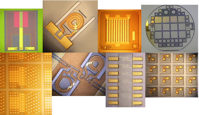
Process development
& Small size production examples
SENSORS
- Radiation (Dosimeter gamma, Photodiodes)
- Chemical ( CHEMFET)
- Thermal (PT100)
- Mechanical
PASSIVES
- Resistors and capacitors
- Yielding components
POWER COMPONENTS
- Si Mosfet (2,4 kV) for military application
- 1 kV Bipolar for static circuit breaker
- 3,3 kV IGBT
On top of traditional semiconductor process steps, IBS has developed specific technology bricks to meet SiC device manufacturing requirement
- Inorganic masking & Hot implantation
- High temperature implant annealing
- Plasma etching
- Fast annealing for metallization
IBS provides you with its skills and its know how to allow you to develop your own component
- Process simulation using SILVACO software
- Process integration
- Electrical simulations
- Design of masks
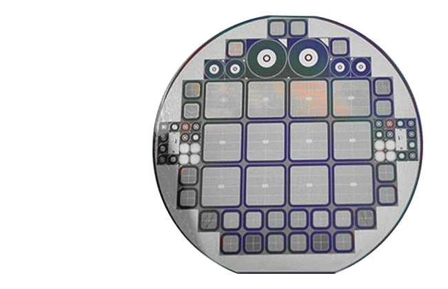
With its production line, IBS can produce components based on you requirement. Our fab operates with 2” to 6” compatible systems
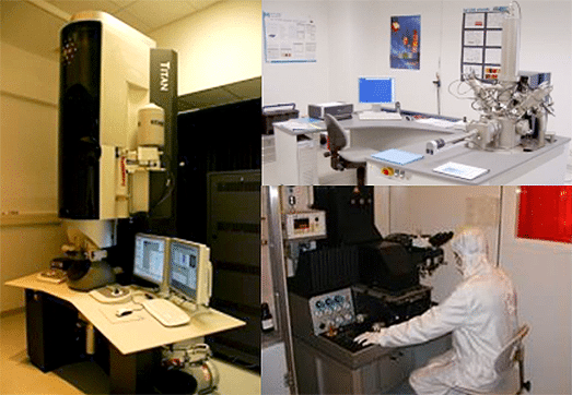
Thanks to the CIMPACA capabilities , IBS can propose a complete set of tools that will perform the following tasks:
ON LINE CHARACTERIZATION:
- mechanical profilometer
- Optical thickness measurment
- Sheet resistance + prober IBS
PHYSICO & DEFCT ANALYSIS:
- D-SIMS & ToF-SIMS
- Micro Auger & XPS
- Dual beam FIB & TEM
- IR Thermography
- Laser decapsulation
OFF LINE CHARACTERIZATION:
- Layers thicknesses & morphology
- Optical 3D Profilometer
- Micro Raman
- AFM Veeco
- SEM
From single step process to complete product
SINGLE STEP PROCESS
- Thin film deposition: PVD (Sputtering), PECVD
- Thermal oxidation & diffusion
- RTA annealing
- Wet (chemical) & dry (RIE) etch
- Photolithography
We operate with a complete semiconductor manufacturing line!