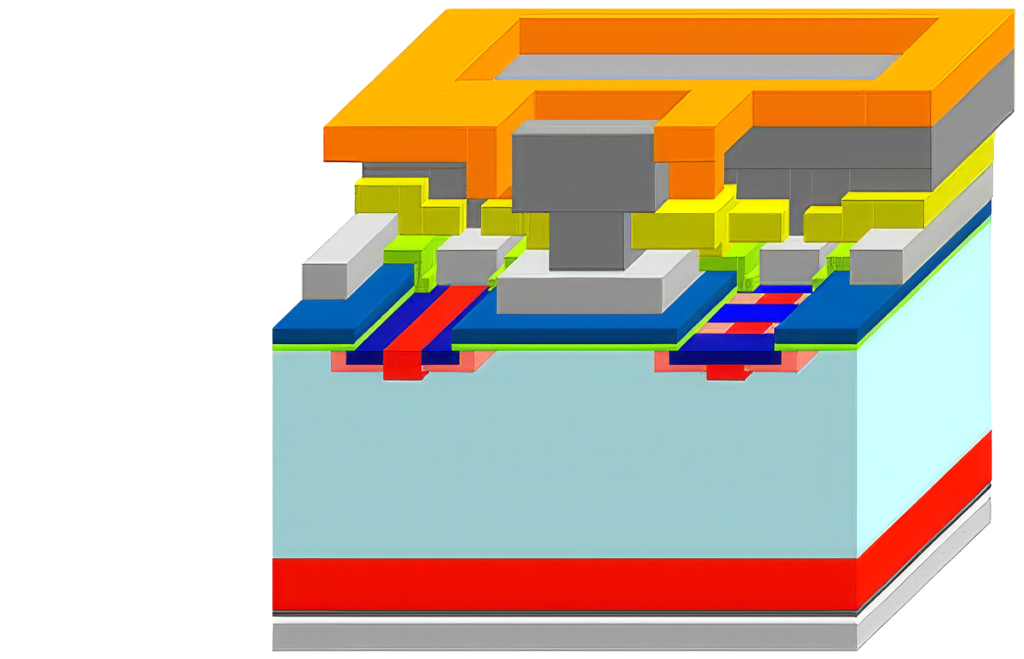
Ion Implantation Foundry Service
IBS is the perfect partner for supporting your ion implantation needs.
Whether it is production or R&D, IBS has a solution to fit all customer’s needs
A new world where Ion implantation is deeply required
- SiC implantation up to 600 °C
- 3D conformal doping
- Surface treatment ( planar to 3D )
IBS is the leading ion implant service
From ultra low energy to high doses on most wafer types and sizes
( Sample to 12" )
with a large variety of species
Plasma immersion ion implantation
- Simultaneous implantation on the whole wafer
- Conformal 3D implantation
- Ultra low energy (down to 30 eV) with no risk of energy contamination
- Hot implant
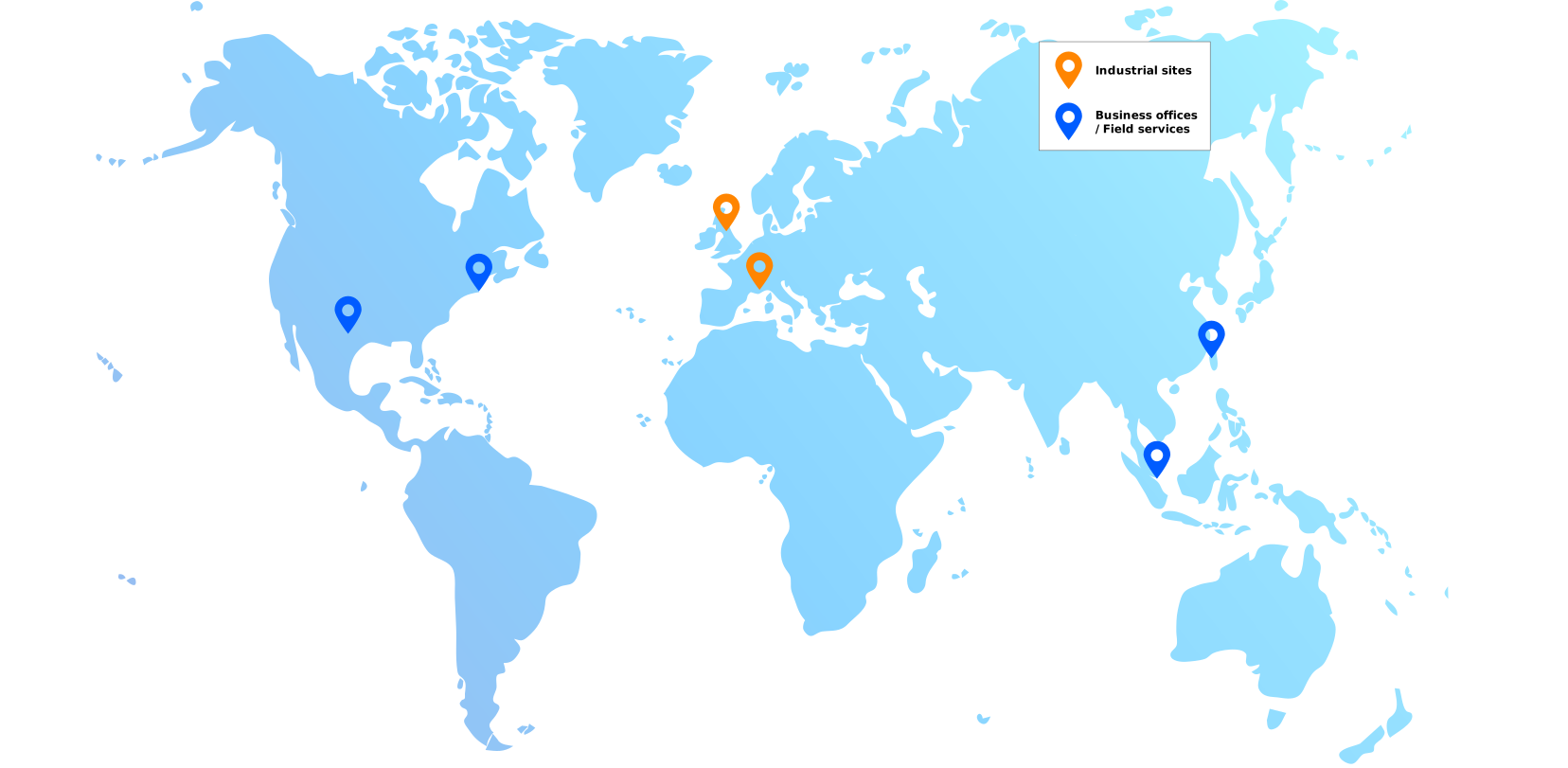
From our two production facilities in France and the UK, IBS operates a world class ion implantation and full process manufacturing line service.
IBS can process production volumes from sample to 12″ diameter substrates, as well as custom shapes, thicknesses and materials.
Request an element
Beamline implantation services
- Standard Processing: Fabless, ion implanter-less or additionnal production capacity without CapEx heavy investment
- Back-up: Breakdown, temporary overlay, wafer size upgrade…
- Specific processes: product development, test & evaluation
- Various substrates, shapes
- Exotic species
- Heated/cooled, various angles…
- From room temperature to +600 °C implant
- From samples to 6” wafer
- Si, B, Al, N, C, P and much more
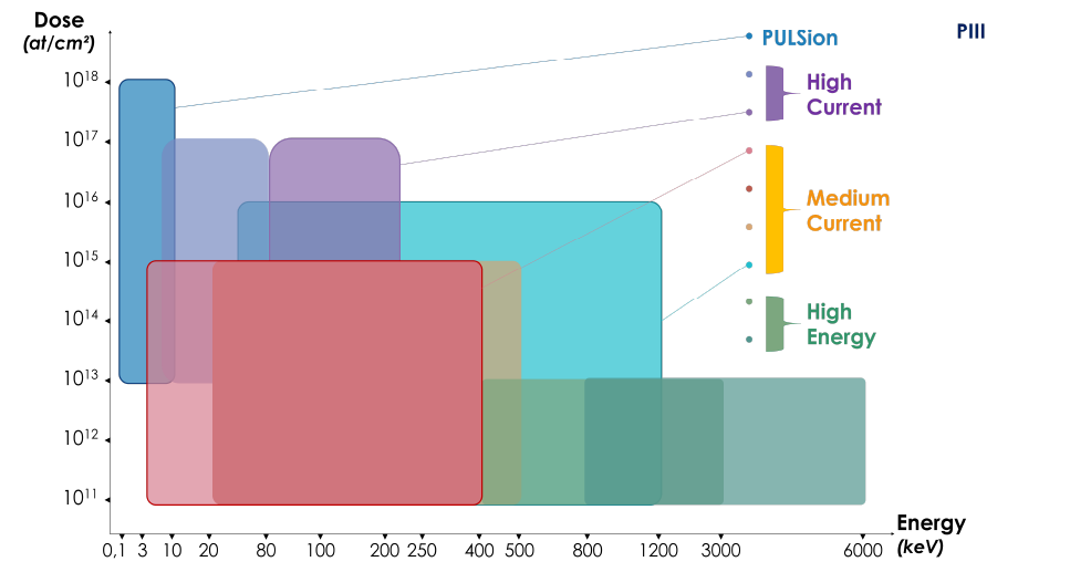
- From 5 to 400 keV
- Specific SiC ion implant simulations
Plasma Immersion Ion Implant services (PIII)
- Available species:
• Doping: AsH3, PH3, BF3, B2H6
• Material modification: Ar, H2, He, CH4, SiH4, SiF4, Al, CF4, C2H2… - Wafer size: from samples up to 300 mm
- From medium to high doses
- Extremely low to medium acceleration voltage: 50 V – 20 kV
- Conformal doping for 3D
- Annealing (and diffusion) depth is controlled very precisely
- Room temperature doping
- Wafer integrity
- Junction depth from 10 nm to 15 nm
- Application: Back side implantation, power components
SCOPE OF WORK
Dose / Energy
Wafer Types
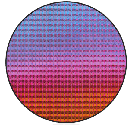
IBS can implant different types of wafers from sample to 12''
- Si
- Si thin wafers / Taiko wafers
- SiC
- GaN
- InP / GaAs
- InSb
- HgCdTe
- LiNbO3
- Sapphire / Diamond / Quartz
Turnkey services
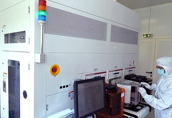
With its line of equipment, IBS can produce ion implantation based on your requirement. Our fab operates with 2” to 300mm compatible systems.
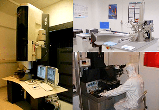
Thanks to its various partnerships, IBS can propose a complete set of metrology tools:
- mechanical profilometer
- Optical thickness measurment
- Sheet resistance + prober IBS
- D-SIMS & ToF-SIMS
- Micro Auger & XPS
- Dual beam FIB & TEM
- IR Thermography
- Laser decapsulation
- Layers thicknesses & morphology
- Optical 3D Profilometer
- Micro Raman
- AFM Veeco
- SEM
IBS provides you with its skills and its know how to allow you to develop your own component
- Process simulation using SILVACO software and IBS in-house SiC implantation simulator