Advanced Ion Implanters

From R&D to High-Volume Production

With 30 years of implant background, IBS is the only company that can offer both a range of new implant tools & full implant services.

Anticipating new technologies

Shaping the 'MORE THAN MOORE' and 'MORE MOORE' frontiers

Ion implantation, essential to those technologies, requires :
  • Higher doses at lower energies with high throughput
  • Implantation of 3D structures
  • Material modification i.e. use of ion implant for non doping applications (etch selectivity, contact improvement, patterning, layer synthesis, strain engineering, etc)
  • Hot implantation
  • Large range of species
Ion implantation tools:
  • High flexibility & versatility
  • High productivity
  • Easy maintenance
  • Low foot print

With 30 years of implant background, IBS is the only company that can offer both a range of new implant tools & full implant services.

0
years of expertise
0
IBS ION IMPLANTERS SOLD
0
DIFFERENT ELEMENTS IMPLANTED

Plasma immersion ion implantation <10 nm

Meet Pulsion®

Plasma Immersion Implantation is a versatile process technology with wide applications in microelectronics processing and materials engineering
PULSION® plasma immersion tool offers:

> Simultaneous implantation of the full wafer
> Ultra low energy (down to 30 eV) with no risk of energy contamination
> Conformal implantation of 3D structures
> Hot implantation
> Wide process range

3D doping (FINFET, DTI, pillars …) for advanced logic & memory
Material modification to tailor stress, to engineer contact & Vt, to help process integration
Very high doses needed for DPG application

IBS PULSION equipment meet < 10 nm requirements

Continued scaling of non-planar HP multigate devices in all aspects:
EOT, junctions, mobility enhancement, new channel materials,
parasitic series resistance, contact silicidation.

• Materials compatibility

• Process integration challenges

Plasma immersion ion implantation <10 nm

FLEXion 200/400 FLEXion 400-SiC

To fulfill manufacturer’s needs for compound Semiconductors and SiC components, IBS has designed a family of implanters avoiding
the costly complexity of a 300 mm Si machine downgraded for SiC.
Key advantages:
  • High beam current
  • Extended life ion source (>300 hrs)
  • Enhanced single or multi-charged Al beam generation
  • High resolution analyzer magnet for multi-charged and high AMU beams
  • 650 °C fast temperature ramp-up/ramp-down platen for SiC
  • Optimized throughput for non Si materials
  • Quad implant, autotune up to 10 chained implantations
  • From coupons to 200 mm, parallel scanning for 200 mm wafers
  • Up to 1.2 MeV
  • High efficiency ion sources (Indirect heated Cathode, ECR)
  • Up to 8 different implant gases
  • Medium current production implanter for:
    RF and power devices, sensors,
  • opto-electronics manufacturing on Si, SiC, GaAs, GaN, LiTaO3, HgCdTe, LiNbO3, InP…

Ion implanters tailored to your needs

Demo Request

Experience the precision of IBS technology before integration.

We invite our customers to validate their specific doping requirements at our state-of-the-art demo facility in Peynier, France. Our experts work closely with your R&D teams to perform process evaluations on your own wafers.

Proof of Concept: Test new ion species or dose recipes.

  • Confidentiality: Secure handling of proprietary designs and materials.

  • Full Characterization: Access to on-site metrology (SIMS, SRP, Metripol) to analyze results immediately.

  • Schedule your demo

    SiC Devices

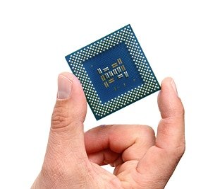
    Silicon carbide (SiC): smaller, faster, more robust, this material will supplant silicon in converters for electrical vehicles, industrial motors and power grids.
    Manufacturing SiC components requires dedicated ion implantation tools.

    IMC advantages

    • Implants up to 800 keV
    • Intense current and stable Al beam
    • High temperature platen

    PULSION® advantages

    • Gate technology engineering for MOS SiC
    • Contact doping improvement

    Customer requirements

    • High temperature implantation
    • Wafer handling for brittle materials

    PULSION® FOR POWER DEVICE APPLICATION

    PULSION® advantages

    • High throughput at high doses and low energy
    • Low-mechanical stress, stable single wafer platen for thinned wafers; reduced breakage
    • Conformal trench sidewall doping (even for high aspect ratio)

    Customer requirements

    • Similar doping results to beamline implantation
    • Higher throughput and performance
    • Possible lower energy control for advanced devices

    Appplications

    • Gate trench sidewall doping (low dose, conformal)
    • Backside contact doping (high dose, after back thinning)
     

    COMPOUND SEMICONDUCTORS

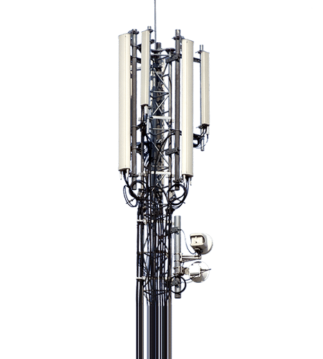
    Data communications, telecommunication systems and security require more and more compound semiconductors such as optoelectronics and RF amplifiers. Due to material and contamination
    concerns, a manufacturing line must operate with dedicated tools.

    IMC advantages

    • 400 kV beam line for implant up to 800 keV
    • Gentle handling for brittle materials
    • Wide range of implant species, among which: Be, Si, Mg, Cs, Yb…

    Typical applications

    • HgCdTe IR sensor and imager
    • InP laser
    • VCSEL
    • GaAs RF power amplifier and switches
    • Power GaN power components

    Implanters Parts retail and maintenance: Access your customer area now

    Your tailored customer area gives you access to our wide parts catalog and order history.

    0
      Your Parts
      No parts yetReturn to Parts

      Login or create a customer area

      For all inquiries, please feel free to reach out at: